Highly coveted in the solar industry: wafer-thin silicon discs
Fraunhofer CSP develops solutions for efficient, cost-effective and reliable solar modules
Emerging from the crisis stronger – this phenomenon should also apply to the solar industry. Under this premise the Fraunhofer Center for Silicon Photovoltaic CSP in Halle carries out applied research throughout the entire process chain for the production of wafer-based silicon solar modules. CSP is taking part in the “Intersolar Europe” trade fair for the solar industry in Munich for the fourth time. This year it has even been nominated for an Innovation Award.
“No, the diamond wire does not sparkle,” sais Stephan Schönfelder, holding it up to the light. The wire looks grey compared to the shiny reddish gold steel wire with brass coating. The diamond coating feels rough and produces a faster dissipation of silicon blocks in the coveted thin wafers. Time is money – with the production of these grey discs that are used as the base plate for solar cells too. Wafer-based silicon solar cells have an 80 percent share of the global production of solar cells and modules. “Roughly a third of the costs for a silicon solar module is accrued before production of the wafer even starts,” says Stephan Schönfelder and he adds that the research is about reducing these costs, even more so due to the crisis on the photovoltaics market. Schönfelder coordinates the research project which the diamond wire saw is involved even in the name: “DiaCell – innovative wafering technologies from the substrate to the photovoltaics module”. The mechanical engineer wrote his doctoral thesis at the Fraunhofer Institute for Mechanics of Materials IWM in Halle. Its theme is based in the field of the mechanics of thin silicon substrates. He is therefore an expert when it comes to the mechanical properties of thin silicon wafers and in producing them in high quality but as cheaply as possible.
Schönfelder holds a disc between his two index fingers. It is roughly 180 micrometres thin, which is the standard, he says, adding that this research project is about producing even thinner silicon wafers, among other things. At the same time they are looking at reducing the breakage rate too. Partners in the project come from regional industry: SILTECTRA from Dresden, bubbles & beyond from Leipzig and Innotech Solar from Halle.
An industry compatible pilot line has been set up at Fraunhofer CSP where the wafers run through the entire production process chain. Existing and new production technologies are tested and optimised here over and over again. As research cannot just rest at having a fantastic idea that changes the intermediate product in the desired way, you also have to look at what influence this idea has on the successive elements in the value chain, says Schönfelder. DiaCell has the job of developing technologies that reduce costs for the entire value chain. As a result, mechanical experiments showed that the diamond wire sawn wafers also have one disadvantage: they break easily in the sawing direction. Furthermore, the diamond wire saw causes chips: very fine powder that contaminates the wafer disc and entails several complex chemical steps in the cleaning process. To save time and money here too, bubbles & beyond is developing so-called “intelligent fluids” together with Fraunhofer CSP. The development of fluids goes hand in hand with the process development and may cut out whole sections in the entire production process in the end.
CSP is researching splitting the wafer without any material loss with the project partner SILTECTRA. After all, every sawing gap causes material loss in the ballpark of one wafer thickness. That is a great deal in relation to the approx. 180 micrometre thin standard disc and may mean up to 50 percent material loss.
With wafer splitting, both sides of the wafer are glued using a special polymer. Once in a frozen state, the plastic film contracts and develops such a force that it pulls the wafer apart.
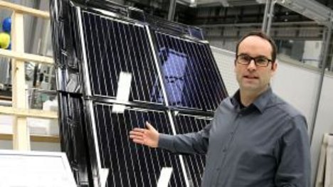
Jens Schneider is standing in front of a structure similar to a roof truss, which solar modules are mounted on. These wafer-based silicon solar cells are not only supposed to capture light but also act as roofing instead of tiles. These kinds of modules are exposed to extreme wear. The doctorate electrical engineer is leading a research project that deals with “modelling the mechanical behaviour of thin silicon substrates and solar cells”. “MechSi”, says Schneider, “is on the one hand investigating what influence new production processes have on the wafer. Whether the wafer-thin silicon discs are made by standard slurry wire saws, diamond wire saws or by splitting, determines their different properties in the end.” Different production processes for the silicon wafer were to be simulated by computer in another work package. And in the third package it is being investigated how the wafer mechanically behaves when being processed into solar cells and modules. Recommended action for companies should result from this. When introducing new processes it is ultimately also about reducing the breakage rate, says Schneider.
Speaking of saving costs and material: even the question of how the quality of solar cells can already be monitored during production is being looked into at Fraunhofer CSP. Crystal defects may cause short circuits in the solar cells and therefore output losses. Potential-induced degradation (PID) is a frequently occurring defect mechanism. PID occurs when solar modules are operated at high system voltages in a damp environment. Together with the company Freiberg Instruments, Fraunhofer CSP has developed a test process plus corresponding device that saves material, energy and costs. PIDcon simplifies and facilitates the quality testing of solar cells and modules. “We are delighted that PIDcon has been nominated for the Intersolar Award 2015,” says Professor Jörg Bagdahn, Head of Fraunhofer CSP in Halle. “Experiences of previous visits to trade fairs have shown that our research expertise is in extremely high demand and that Intersolar gives us access to important contacts with manufacturers, suppliers and other partners in the industry.”
Image caption: Jens Schneider, manager of the “Modelling the mechanical behaviour of thin silicon substrates and solar cells” research project presents solar modules that replace roof tiles.