
© Fraunhofer IMWS
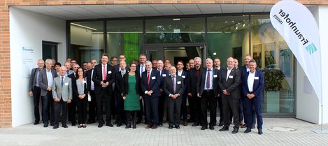
New equipment, new laboratories: Opening ceremony of the extension building
With the expansion of the Fraunhofer Center for Applied Microstructure Diagnostics CAM, the Fraunhofer Institute for Microstructures of Materials and Systems IMWS in Halle (Saale) is expanding its leading international position in the field of microstructure diagnostics. With new equipment and new premises, the building opened today offers even better possibilities for investigating materials down to the atomic level and thus, for example, increasing the safety and service life of components for autonomous driving. A total of 9.9 million euros was invested in this project.
"What Went Wrong? ("Where is the mistake?") is the lettering that artist Michael Krenz affixed to the wall of the new building. This is precisely the question Fraunhofer CAM employees are investigating with a view to materials and components for electronics as well as optical materials and technologies: Using the latest diagnostic methods and state-of-the-art analytical equipment, they investigate how defects arise, what changes occur in the microstructure of materials during production and use, and how more efficient materials can be developed.
"Components for new assistance systems in automotive engineering, for example, can only function properly if the behavior of the materials used is understood down to the smallest detail. We deliver this know-how to our customers. With these additional possibilities, we are once again raising the expertise in microstructure elucidation traditionally available in Halle to a new level. I am very pleased about this and would like to thank everyone who contributed to the expansion of the Fraunhofer CAM," says Prof. Ralf B. Wehrspohn, Director of the Fraunhofer IMWS, at the opening of the building.
Dr. Reiner Haseloff, Minister President of the State of Saxony-Anhalt, emphasized the contribution the research facility makes to important future topics such as digitization, new mobility concepts and energy-efficient and CO2-reduced manufacturing processes: "With its internationally recognized expertise, the Fraunhofer CAM not only supports world-class corporations, but also hidden champions in the region. The expansion will create an even better interface between scientific excellence and industrial users. This will enable us to tap growth potential in key technologies."
Since construction began in February 2017, 778 m2 of additional floor space has been created. In the course of the expansion, 25 new high-tech jobs were created. The total costs amount to around 9.9 million euros, of which around 4.5 million euros were invested in new equipment technology.
These include a probe-corrected high-resolution transmission electron microscope, the first instrument of this performance class in Europe, a time-of-flight secondary ion mass spectrometer for surface analysis and a scanning electron microscope for nanoprobing that can be combined with focusing ion beam technology. "With this expanded equipment pool, we are at the global forefront of technology and are expanding our unique selling propositions. On the one hand, we can meet the considerably increased demand of our customers, who rely on us as their partner to meet the highest safety and reliability requirements. On the other hand, we now have the best conditions to develop new and more efficient material and defect analysis techniques together with the equipment manufacturers," says Prof. Matthias Petzold, head of the "Materials and Components for Electronics" business unit. He underlines the importance of quality assurance of electronic components, not only for autonomous driving or electric mobility: "Without reliable electronics, the challenges of digitization or improved resource efficiency cannot be mastered".
The "Optical Materials and Technologies" business unit of the Fraunhofer IMWS, founded in 2018, will also find its new home in the expanded building. There, high-tech components and nanotechnology materials will be investigated and further developed, particularly for highly complex optical applications such as mirrors for extreme ultraviolet light, modern spectacle lenses, glass ceramics and effect paints. "Such applications are based on complex layer systems consisting of only a few atomic layers or nanostructured components. Highest-resolution analytics are indispensable for mastering manufacturing processes or assessing the market potential of new solutions," says Prof. Thomas Höche, head of the business unit. "Just as materials are constantly changing and becoming more efficient, so too must our analytical tools and methods. We are excellently positioned for this at the new Fraunhofer CAM."